Program
10:00 Walk-in and Innovation Market
10:30 Welcome and opening

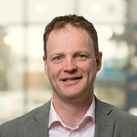
10:45 Panel discussion


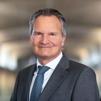
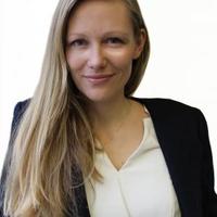
Marc Hijink, journalist and author of FOCUS: the world of ASML, hosts a panel discussion on the challenges of the Dutch semicon industry.
11:30 Keynote Samsung
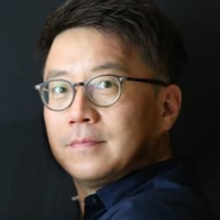
We will discuss the role and challenge of MI. Various spectrum ranges in H/W have been attempted to be used to overcome the challenge. In the methodology the MI role is expanding to quality prediction by extracting hidden meaning with the help of AI technology, finally combining the MI role will expand for cognitive prediction and preventive action in the future.
11:45 Break
12:15 Keynote ASM

Artificial intelligence will drive a transition toward 3D architectures and lower power consumption, which in turn will need many advanced materials and deposition process innovations. ASM will address these opportunities in a sustainable way.
12:45 Keynote ASML
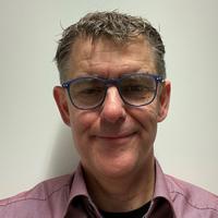
During the presentation the need from the semiconductor industry will be described generically. This will be translated to the future product portfolio of ASML. Based on that the technical challenges will be touched upon. It will be made clear that this requires a balancing act to create such a complex system taking into account requirements, regulations and policies.
13:15 Lunch, networking and Innovation Market
14:15 Breakout sessions round 1
14:15 Metrology and testing

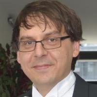
Presentation Aleksandar Andreski: MEMS & Photonic Testing - Production testing of silicon devices in the More-than-Moore category is often not trivial due to various probing and measurement challenges. Salland together with partners has been developing new equipment and methods to improve production testing of specifically Photonic and MEMS devices. In this talk we shortly present our progress in this area.
14:15 Public funding opportunities in the European Union and the Netherlands
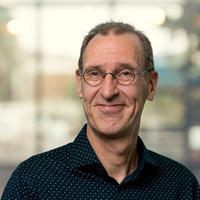
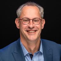

Public funding opportunities in the European Union and the Netherlands
14:15 Sustainability
Presentation Joe Trimboli: Advanced Materials for PFAS-Free Applications
15:15 Breakout sessions round 2
15:15 Acoustic and E-beam Metrology
Presentation Benoit Quesson: GHz half wavelength contact acoustic microscopy (HaWaCAM) - HaWaCAM is a new acoustical metrology technique developed by TNO using GHz scattering acoustics, the promising results indicate a strong potential for semiconductor inspection and metrology applications
Presentation Jacob Hoogenboom:Perspectives and challenges for electron-beam metrology - Electron microscopy offers nanometer resolution but also faces challenges that hamper routine application in semiconductor metrology. I will discuss these challenges and present some of our approaches towards tackling these from both a fundamental and an engineering perspective.
15:15 Future Mechatronic System Architecture Developments for Semicon Equipment
15:15 Quantum Technology


Presentation Clara Osorio: Quantum Sensing - We live in a world of sensors constantly translating stimuli into electric signals. Whether it’s the thermometers in our homes, the high-performance sensors in our smartphones, or the myriad sensors within the machinery fabricating such devices. As their ubiquity is undeniable, the impact of better sensors might be extensive and unexpected. During this talk, I will introduce Quantum Sensors, a type of sensor where a coherent transformation of quantum systems mediates the sensing process. I will provide examples of their use and describe TNO's and QDNL's programs aimed at accelerating their industrialization.
Presentation Fokko de Vries: Enabling useful quantum computing - Quantum computations that are useful for chemistry, material science and life science require at least a thousand to a million qubits. In order to perform operations on these qubits, Qblox has developed a highly distributed control architecture where each module executes control or readout operations on a small number of qubits. This entails sending real time sequences of electronic pulses and performing measurement operations. As a result, the control stack processes 1000s of outgoing and incoming pulses in full synchronicity while operating with minimal precompilation and communication overhead. This scalable solution is a key enabling technology to move quantum computers from the lab to useful applications.
